Thursday, September 29, 2022

Computer Organization and Architecture (Solved Answers from QBank - IX) - Tirthankar Pal - MBA from IIT Kharagpur, GATE, GMAT, IIT Written Test, Interview were a part of MBA Entrance, B.S. in Computer Science from NIELIT


Distinguish between synchronous and asynchronous DRAMS 

The key difference between synchronous and asynchronous DRAM is that the synchronous DRAM uses the system clock to coordinate the memory access while asynchronous DRAM does not use the system clock to coordinate the memory access.

The computer memory stores data and instructions. There are mainly two types of memory called RAM and ROM. RAM stands for Random Access Memory while ROM stands for Read Only Memory. The RAM further divides into static RAM and dynamic RAM. This article discusses two types of dynamic RAM namely, synchronous and asynchronous DRAM.

CONTENTS

1. Overview and Key Difference
2. What is Synchronous DRAM
3. What is Asynchronous DRAM
4. Side by Side Comparison – Synchronous vs Asynchronous DRAM in Tabular Form
5. Summary

What is Synchronous DRAM?

RAM is a volatile memory. In other words, the data and instructions written to the RAM are not permanent. Therefore, the data will erase when power off the computer. It is possible to perform both read and write operations in RAM. Moreover, it is fast and expensive. There are two types of RAM. They are the Static RAM (SRAM) and Dynamic RAM (DRAM).  The SRAM requires a constant flow of power to retain data while DRAM requires constant refreshes to retain data. Synchronous DRAM and Asynchronous DRAM are two types of DRAM.

Difference Between Synchronous and Asynchronous DRAM

Figure 01: SDRAM

In Synchronous DRAM, the system clock coordinates or synchronizes the memory accessing. Therefore, the CPU knows the timing or the exact number of cycles in which the data will be available from the RAM to the input, output bus.  It increases memory read and write speed. Overall, the Synchronous DRAM is faster in speed and operates efficiently than the normal DRAM.

What is Asynchronous DRAM?

The first personal computers used asynchronous DRAM. It is an older version of DRAM. In asynchronous DRAM, the system clock does not coordinate or synchronizes the memory accessing. When accessing the memory, the value appears on the input, output bus after a certain period. Therefore, it has some latency that minimizes the speed.

Usually, asynchronous RAM works in low-speed memory systems but not appropriate for modern high-speed memory systems. At present, the manufacturing of asynchronous RAM is quite low. Today, synchronous DRAM is used instead of the asynchronous DRAM.


What is the Difference Between Synchronous and Asynchronous DRAM?

Synchronous DRAM uses a system clock to coordinate memory accessing while Asynchronous DRAM does not use a system clock to synchronize or coordinate memory accessing. Synchronous DRAM is faster and efficient then asynchronous DRAM.

Furthermore, synchronous DRAM provides high performance and better control than the asynchronous DRAM. Modern high-speed PCs uses synchronous DRAM while older low-speed PCs used asynchronous DRAM.

Difference Between Synchronous and Asynchronous DRAM in Tabular Form

Summary – Synchronous vs Asynchronous DRAM

The difference between synchronous and asynchronous DRAM is that synchronous DRAM uses the system clock to coordinate the memory access while asynchronous DRAM does not use the system clock to coordinate the memory accessing. In brief, the synchronous DRAM provides better control and high performance than the asynchronous DRAM.

Bus transactions on PCI

Let's look at what happens during a PCI data transfer or bus transaction. First, the initiating device has to get permission to have control of the bus. This is determined during the process of bus arbitration. A function called the arbiter, which is part of the PCI chip set, decides which device is allowed to initiate a transaction next. The arbiter uses an algorithm designed to avoid deadlocks and prevent one or more devices from monopolising the bus to the exclusion of others.


Having gained control of the bus, an initiator then places the target address and a code representing the transfer type on the bus. Other PCI devices determine, by decoding the address and the command type information, whether they are the intended target for the transfer. The target device claims the transaction by asserting a device select signal.


Once the target has sent its acknowledgement, the bus transaction enters the data phase. During this phase the data is transferred. The transfer can be terminated either by the initiator, when the transfer is completed or when its permission to use the bus is withdrawn by the arbiter, or by the target if it is unable to accept any more data for the time being. If the latter, the transfer must be restarted as a separate transaction. One of the rules of PCI protocol is that a target must terminate a transaction and release the bus if it is unable to process any more data, so a slow target device cannot hog the bus and prevent others from using it.


Note that although all PCI data transfers are burst transfers, a device does not have to be able to accept long bursts of data. A target device can terminate the data phase after one cycle if it wants to. Such behaviour would be perfectly acceptable in a non-performance-critical device. Even high performance devices may have to terminate a burst, since their data buffers will be of finite size and if they cannot process the data as quickly as it is sent these buffers will eventually fill up.


Tirthankar Pal

MBA from IIT Kharagpur with GATE, GMAT, IIT Kharagpur Written Test, and Interview

2 year PGDM (E-Business) from Welingkar, Mumbai

4 years of Bachelor of Science (Hons) in Computer Science from the National Institute of Electronics and Information Technology

Google and Hubspot Certification

Brain Bench Certification in C++, VC++, Data Structure and Project Management

10 years of Experience in Software Development out of that 6 years 8 months in Wipro

Selected in Six World Class UK Universities:-

King's College London, Durham University, University of Exeter, University of Sheffield, University of Newcastle, University of Leeds


Computer Organization and Architecture (Solved Answers from QBank - VIII) - Tirthankar Pal - MBA from IIT Kharagpur, GATE, GMAT, IIT Written Test, Interview were a part of MBA Entrance, B.S. in Computer Science from NIELIT

Bus Arbitration

Bus Arbitration refers to the process by which the current bus master accesses and then leaves the control of the bus and passes it to another bus requesting processor unit. The controller that has access to a bus at an instance is known as a Bus master

A conflict may arise if the number of DMA controllers or other controllers or processors try to access the common bus at the same time, but access can be given to only one of those. Only one processor or controller can be Bus master at the same point in time. To resolve these conflicts, the Bus Arbitration procedure is implemented to coordinate the activities of all devices requesting memory transfers. The selection of the bus master must take into account the needs of various devices by establishing a priority system for gaining access to the bus. The Bus Arbiter decides who would become the current bus master. 

There are two approaches to bus arbitration:  

  1. Centralized bus arbitration – 
    A single bus arbiter performs the required arbitration. 
     
  2. Distributed bus arbitration – 
    All devices participating in the selection of the next bus master. 

Methods of Centralized BUS Arbitration: 

There are three bus arbitration methods: 

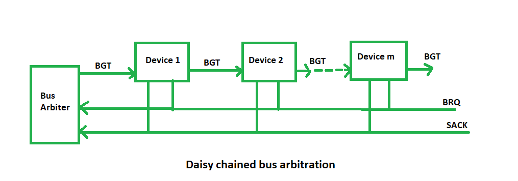
(i) Daisy Chaining method: It is a simple and cheaper method where all the bus masters use the same line for making bus requests. The bus grant signal serially propagates through each master until it encounters the first one that is requesting access to the bus. This master blocks the propagation of the bus grant signal, therefore any other requesting module will not receive the grant signal and hence cannot access the bus.
During any bus cycle, the bus master may be any device – the processor or any DMA controller unit, connected to the bus. 

Advantages: 

  • Simplicity and Scalability.
  • The user can add more devices anywhere along the chain, up to a certain maximum value. 

Disadvantages:

  • The value of priority assigned to a device depends on the position of the master bus.
  • Propagation delay arises in this method.
  • If one device fails then the entire system will stop working. 
     

(ii) Polling or Rotating Priority method: In this, the controller is used to generate the address for the master(unique priority), the number of address lines required depends on the number of masters connected in the system. The controller generates a sequence of master addresses. When the requesting master recognizes its address, it activates the busy line and begins to use the bus.


Advantages – 

  • This method does not favor any particular device and processor.
  • The method is also quite simple.
     

Disadvantages – 

  • Adding bus masters is difficult as increases the number of address lines of the circuit.
  • If one device fails then the entire system will not stop working. 

(iii) Fixed priority or Independent Request method – 
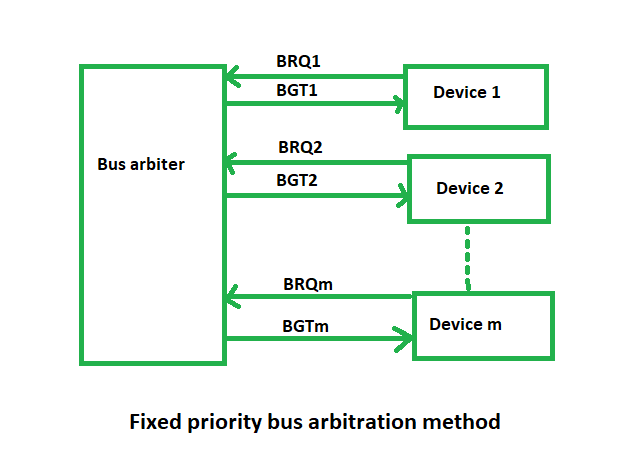
In this, each master has a separate pair of bus request and bus grant lines and each pair has a priority assigned to it.  

The built-in priority decoder within the controller selects the highest priority request and asserts the corresponding bus grant signal.


Advantages – 

  • This method generates a fast response.

Disadvantages – 

  • Hardware cost is high as a large no. of control lines is required. 
     

Distributed BUS Arbitration :
In this, all devices participate in the selection of the next bus master. Each device on the bus is assigned a 4bit identification number. The priority of the device will be determined by the generated ID.


Set Associative Cache Mapping


Set-associative Mapping –
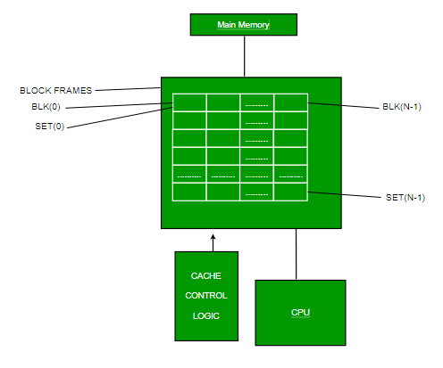
This form of mapping is an enhanced form of direct mapping where the drawbacks of direct mapping are removed. Set associative addresses the problem of possible thrashing in the direct mapping method. It does this by saying that instead of having exactly one line that a block can map to in the cache, we will group a few lines together creating a set. Then a block in memory can map to any one of the lines of a specific set..Set-associative mapping allows that each word that is present in the cache can have two or more words in the main memory for the same index address. Set associative cache mapping combines the best of direct and associative cache mapping techniques.

In this case, the cache consists of a number of sets, each of which consists of a number of lines. The relationships are

m = v * k
i= j mod v

where
i=cache set number
j=main memory block number
v=number of sets
m=number of lines in the cache number of sets 
k=number of lines in each set 

Application of Cache Memory –

  1. Usually, the cache memory can store a reasonable number of blocks at any given time, but this number is small compared to the total number of blocks in the main memory.
  2. The correspondence between the main memory blocks and those in the cache is specified by a mapping function.


Types of Cache –

  • Primary Cache –
    A primary cache is always located on the processor chip. This cache is small and its access time is comparable to that of processor registers.
  • Secondary Cache –
    Secondary cache is placed between the primary cache and the rest of the memory. It is referred to as the level 2 (L2) cache. Often, the Level 2 cache is also housed on the processor chip.


Locality of reference –
Since size of cache memory is less as compared to main memory. So to check which part of main memory should be given priority and loaded in cache is decided based on locality of reference.

Types of Locality of reference

  1. Spatial Locality of reference
    This says that there is a chance that element will be present in the close proximity to the reference point and next time if again searched then more close proximity to the point of reference.
  2. Temporal Locality of reference
    In this Least recently used algorithm will be used. Whenever there is page fault occurs within a word will not only load word in main memory but complete page fault will be loaded because spatial locality of reference rule says that if you are referring any word next word will be referred in its register that’s why we load complete page table so the complete block will be loaded.

Tirthankar Pal

MBA from IIT Kharagpur with GATE, GMAT, IIT Kharagpur Written Test, and Interview

2 year PGDM (E-Business) from Welingkar, Mumbai

4 years of Bachelor of Science (Hons) in Computer Science from the National Institute of Electronics and Information Technology

Google and Hubspot Certification

Brain Bench Certification in C++, VC++, Data Structure and Project Management

10 years of Experience in Software Development out of that 6 years 8 months in Wipro

Selected in Six World Class UK Universities:-

King's College London, Durham University, University of Exeter, University of Sheffield, University of Newcastle, University of Leeds


Computer Organization and Architecture (Solved Answers from QBank - VII) - Tirthankar Pal - MBA from IIT Kharagpur, GATE, GMAT, IIT Written Test, Interview were a part of MBA Entrance, B.S. in Computer Science from NIELIT

Direct Memory Access (DMA) :

DMA Controller is a hardware device that allows I/O devices to directly access memory with less participation of the processor. DMA controller needs the same old circuits of an interface to communicate with the CPU and Input/Output devices. 

Fig-1 below shows the block diagram of the DMA controller. The unit communicates with the CPU through data bus and control lines. Through the use of the address bus and allowing the DMA and RS register to select inputs, the register within the DMA is chosen by the CPU. RD and WR are two-way inputs. When BG (bus grant) input is 0, the CPU can communicate with DMA registers. When BG (bus grant) input is 1, the CPU has relinquished the buses and DMA can communicate directly with the memory.

DMA controller registers :

The DMA controller has three registers as follows.

  • Address register – It contains the address to specify the desired location in memory.
  • Word count register – It contains the number of words to be transferred.
  • Control register – It specifies the transfer mode.

Note – 

All registers in the DMA appear to the CPU as I/O interface registers. Therefore, the CPU can both read and write into the DMA registers under program control via the data bus.

Fig 1- Block Diagram

Explanation :

The CPU initializes the DMA by sending the given information through the data bus.

  • The starting address of the memory block where the data is available (to read) or where data are to be stored (to write).
  • It also sends word count which is the number of words in the memory block to be read or write.
  • Control to define the mode of transfer such as read or write.
  • A control to begin the DMA transfer.

Burst Mode –

  • In this mode Burst of data (entire data or burst of block containing data) is transferred before CPU takes control of the buses back from DMAC.
  • This is the quickest mode of DMA Transfer since at once a huge amount of data is being transferred.
  • Since at once only the huge amount of data is being transferred so time will be saved in huge amount.

Percentage of Time CPU remains blocked :
Let time taken to prepare the data be Tx and time taken to transfer the data be Ty. Then percentage of time CPU remains blocked due to DMA is as follows.

Percentage of time CPU remains in blocked state = Ty * 100% / Tx + Ty

Tirthankar Pal

MBA from IIT Kharagpur with GATE, GMAT, IIT Kharagpur Written Test, and Interview

2 year PGDM (E-Business) from Welingkar, Mumbai

4 years of Bachelor of Science (Hons) in Computer Science from the National Institute of Electronics and Information Technology

Google and Hubspot Certification

Brain Bench Certification in C++, VC++, Data Structure and Project Management

10 years of Experience in Software Development out of that 6 years 8 months in Wipro

Selected in Six World Class UK Universities:-

King's College London, Durham University, University of Exeter, University of Sheffield, University of Newcastle, University of Leeds


Computer Organization and Architecture (Solved Answers from QBank = VI) - Tirthankar Pal - MBA from IIT Kharagpur, GATE, GMAT, IIT Written Test, Interview were a part of MBA Entrance, B.S. in Computer Science from NIELIT

Why do dynamic Rams need constant refreshing?

Why refresh?


DRAM uses capacitors as storage cells. These capacitors, being really small and made from silicon, will leak off their voltage over time. That’s the D in DRAM: the cells are dynamic: their charge state changes.


To preserve the logic state of those leaky DRAM cells, their state must be read before their charge has bled off, then written back to bring their state to full, freshly-written charge. That’s refresh, in a nutshell.


To help deal with this, DRAMs implement a special kind of read-then-write cycle, called refresh, that hits multiple cells at once and writes them back. Typically, this is one or more rows of cells, about 1/256th of the DRAM at a time.


The host refresh operation is a race against time: all the DRAM rows have to be hit in time before their contents leak away. This usually works out to between 8 and 16ms to hit all the rows.

In contrast, Static RAM, or SRAM, uses a latch as a storage element. The latch keeps its state as long as the power is kept on or it’s written with a new value.


What does this mean with power and density?


SRAM can, in theory, have almost no standby power, as it uses a CMOS latch to store data. In practice, fast SRAM will have fairly high standby leakage current and even higher current during activity due to the use of low-threshold transistors to increase speed.


SRAM latches take between 4 and 8 transistors per bit, and all of them can leak.


Meanwhile, DRAM has standby power to deal with refreshes. There’s considerable effort by chipmakers to offer low-power self-refresh modes that both stretches out the time between each refresh operation, and doesn’t require host intervention once that mode is entered. This self-refresh mode gets used in computer ‘sleep’ state, allowing CPU power-down yet enabling near-instant wake up time.


Density-wise, DRAM basically uses one transistor per cell, connecting to the capacitor which is dug vertically as a well into the silicon. This makes DRAM area per bit very small compared to the SRAM 6T or 8T latch cell. With fewer transistors, DRAM standby leakage per bit is also reduced.


So overall, owing to its density and lower transistor count per bit, DRAM is substantially better power than fast SRAM; but substantially worse than slow, low-leakage SRAM because it requires refreshing.


How DRAM refresh works

While the memory is operating, each memory cell must be refreshed repetitively, within the maximum interval between refreshes specified by the manufacturer, which is usually in the millisecond region. Refreshing does not employ the normal memory operations (read and write cycles) used to access data, but specialized cycles called refresh cycles which are generated by separate counter circuits in the memory circuitry and interspersed between normal memory accesses.


The storage cells on a memory chip are laid out in a rectangular array of rows and columns. The read process in DRAM is destructive and removes the charge on the memory cells in an entire row, so there is a row of specialized latches on the chip called sense amplifiers, one for each column of memory cells, to temporarily hold the data. During a normal read operation, the sense amplifiers after reading and latching the data, rewrite the data in the accessed row before sending the bit from a single column to output. This means the normal read electronics on the chip can refresh an entire row of memory in parallel, significantly speeding up the refresh process. A normal read or write cycle refreshes a row of memory, but normal memory accesses cannot be relied on to hit all the rows within the necessary time, necessitating a separate refresh process. Rather than use the normal read cycle in the refresh process, to save time an abbreviated cycle called a refresh cycle is used. The refresh cycle is similar to the read cycle, but executes faster for two reasons:

  • For a refresh, only the row address is needed, so a column address doesn't have to be applied to the chip address circuits.
  • Data read from the cells does not need to be fed into the output buffers or the data bus to send to the CPU.

The refresh circuitry must perform a refresh cycle on each of the rows on the chip within the refresh time interval, to make sure that each cell gets refreshed.

Types of refresh circuits

Although in some early systems the microprocessor controlled refresh, with a timer triggering a periodic interrupt that ran a subroutine that performed the refresh, this meant the microprocessor could not be paused, single-stepped, or put into energy-saving hibernation without stopping the refresh process and losing the data in memory. So in modern systems refresh is handled by circuits in the memory controller, which may be embedded in the chip itself. Some DRAM chips, such as pseudostatic RAM (PSRAM), have all the refresh circuitry on the chip, and function like static RAM as far as the rest of the computer is concerned.

Usually the refresh circuitry consists of a refresh counter which contains the address of the row to be refreshed which is applied to the chip's row address lines, and a timer that increments the counter to step through the rows. This counter may be part of the memory controller circuitry, or on the memory chip itself. Two scheduling strategies have been used:

  • Burst refresh - a series of refresh cycles are performed one after another until all the rows have been refreshed, after which normal memory accesses occur until the next refresh is required
  • Distributed refresh - refresh cycles are performed at regular intervals, interspersed with memory accesses.

Burst refresh results in long periods when the memory is unavailable, so distributed refresh has been used in most modern systems, particularly in real time systems. In distributed refresh, the interval between refresh cycles is

For example, DDR SDRAM has a refresh time of 64 ms and 8,192 rows, so the refresh cycle interval is 7.8 Î¼s.

Recent generations of DRAM chips contain an integral refresh counter, and the memory control circuitry can either use this counter or provide a row address from an external counter. These chips have three standard ways to provide refresh, selected by different patterns of signals on the "column select" (CAS) and "row select" (RAS) lines:

  • "RAS only refresh" - In this mode the address of the row to refresh is provided by the address bus lines, so it is used with external counters in the memory controller.
  • "CAS before RAS refresh" (CBR) - In this mode the on-chip counter keeps track of the row to be refreshed and the external circuit merely initiates the refresh cycles.[5] This mode uses less power because the memory address bus buffers don't have to be powered up. It is used in most modern computers.
  • "Hidden refresh" - This is an alternate version of the CBR refresh cycle which can be combined with a preceding read or write cycle.[5] The refresh is done in parallel during the data transfer, saving time.

Since the 2012 generation of DRAM chips, the "RAS only" mode has been eliminated, and the internal counter is used to generate refresh. The chip has an additional sleep mode, for use when the computer is in sleep mode, in which an on-chip oscillator generates internal refresh cycles so that the external clock can be shut down.

Refresh overhead

The fraction of time the memory spends on refresh, the refresh overhead, can be calculated from the system timing:

For example, an SDRAM chip has 213 = 8,192 rows, a refresh interval of 64 ms, the memory bus runs at 133 MHz, and the refresh cycle takes 4 clock cycles. The time for a refresh cycle is

So less than 0.4% of the memory chip's time will be taken by refresh cycles. In SDRAM chips, the memory in each chip is divided into banks which are refreshed in parallel, saving further time. So the number of refresh cycles needed is the number of rows in a single bank, given in the specifications, which in the 2012 generation of chips has been frozen at 8,192.

Refresh interval

The maximum time interval between refresh operations is standardized by JEDEC for each DRAM technology, and is specified in the manufacturer's chip specifications. It is usually in the range of milliseconds for DRAM and microseconds for eDRAM. For DDR2 SDRAM chips it is 64 ms. It depends on the ratio of charge stored in the memory cell capacitors to leakage currents. Despite the fact that the geometry of the capacitors has been shrinking with each new generation of memory chips, so later generation capacitors store less charge, refresh times for DRAM have been improving; from 8 ms for 1M chips, 32 ms for 16M chips, to 64 ms for 256M chips. This improvement is achieved mainly by developing transistors that cause significantly less leakage. Longer refresh time means a smaller fraction of the device's time is occupied with refresh, leaving more time for memory accesses. Although refresh overhead occupied up to 10% of chip time in earlier DRAMs, in modern chips this fraction is less than 1%.

Because the leakage currents in semiconductors increase with temperature, refresh times must be decreased at high temperature. DDR2 SDRAM chips have a temperature-compensated refresh structure; refresh cycle time must be halved when chip case temperature exceeds 85 °C (185 °F).

The actual persistence of readable charge values and thus data in most DRAM memory cells is much longer than the refresh time, up to 1–10 seconds. However transistor leakage currents vary widely between different memory cells on the same chip due to process variation. In order to make sure that all the memory cells are refreshed before a single bit is lost, manufacturers must set their refresh times conservatively short.

This frequent DRAM refresh consumes a third of the total power drawn by low-power electronics devices in standby mode. Researchers have proposed several approaches for extending battery run-time between charges by reducing the refresh rate, including temperature-compensated refresh (TCR) and retention-aware placement in DRAM (RAPID). Experiments show that in a typical off-the-shelf DRAM chip, only a few weak cells really require the worst-case 64 ms refresh interval,[13] and even then only at the high end of its specified temperature range. At room temperature (e.g. 24 °C (75 °F)), those same weak cells need to be refreshed once every 500 ms for correct operation. If the system can avoid using the weakest 1% of pages, a typical DRAM only needs to be refreshed once a second, even at 70 °C (158 °F), for correct operation of the remaining 99% of the pages. Some experiments combine these two complementary techniques, giving correct operation at room temperature at refresh intervals of 10 seconds.[13]

For error-tolerant applications (e.g. graphics applications), refreshing non-critical data stored in DRAM or eDRAM at a rate lower than their retention period saves energy with minor quality loss, which is an example of approximate computing.


Tirthankar Pal

MBA from IIT Kharagpur with GATE, GMAT, IIT Kharagpur Written Test, and Interview

2 year PGDM (E-Business) from Welingkar, Mumbai

4 years of Bachelor of Science (Hons) in Computer Science from the National Institute of Electronics and Information Technology

Google and Hubspot Certification

Brain Bench Certification in C++, VC++, Data Structure and Project Management

10 years of Experience in Software Development out of that 6 years 8 months in Wipro

Selected in Six World Class UK Universities:-

King's College London, Durham University, University of Exeter, University of Sheffield, University of Newcastle, University of Leeds